Pseudo-halide buried interface engineering for high-mobility 2D tin perovskite transistors exhibiting enhanced photonic synaptic functionality
This study explores pseudo-halide buried interface engineering using Sn(SCN)₂, Pb(SCN)₂, and Sn(Ac)₂ seed layers to optimize two-dimensional (2D) tin-based perovskite transistors. While Sn-based perovskites offer low toxicity and high charge transport potential, they typically suffer from Sn vacancies, oxidation instability, and poor interface quality. Introducing these interfacial seed layers effectively regulates crystallization dynamics and suppresses Sn²⁺ oxidation. Consequently, the Sn(SCN)₂-modified transistor achieves an outstanding hole mobility of 6.40 cm²V⁻¹s⁻¹ and exhibits strongly enhanced green-light-stimulated photonic synaptic functionalities without requiring a complex heterojunction design.
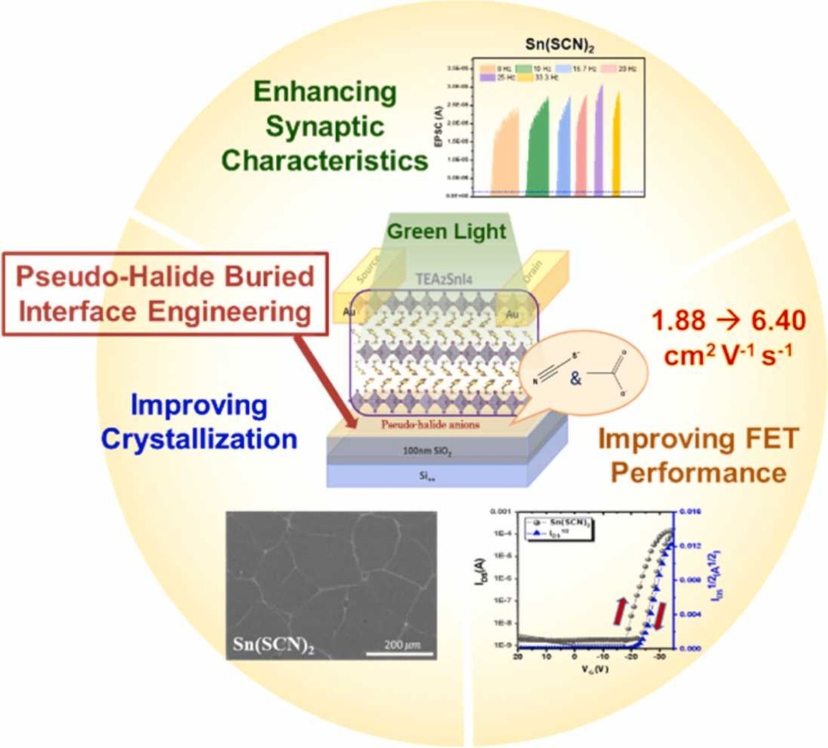
Graphical Abstract.
Technology Overview
Pseudo-halide seed layers are introduced at the buried perovskite/dielectric interface. The anions act as Lewis bases that coordinate with Sn ions to passivate deep trap states, retard crystallization rates, and promote larger grain formation. This reduces non-radiative recombination and p-type self-doping while aligning energy levels to lower hole injection barriers.
Applications & Benefits
This technology is highly applicable to next-generation flexible optoelectronics, neuromorphic computing, and artificial intelligence hardware. It delivers remarkable environmental benefits by utilizing non-toxic tin instead of lead. Mechanically, it yields superior operational stability, high carrier mobility, and energy-efficient, single-layer photonic synapses capable of mimicking advanced short- and long-term biological memory functions.
Abstract:
Two-dimensional (2D) Sn-based perovskites combine low toxicity with excellent charge transport, making them promising candidates for next-generation optoelectronic and neuromorphic devices. However, their performance is often constrained by inherent defects, oxidation instability, and suboptimal interface quality of the films. This study demonstrates that pseudo-halide buried interface engineering [using Sn(SCN)₂, Pb(SCN)₂, and Sn(Ac)₂ as seed layers] significantly enhances the performance of 2D Sn-perovskite transistors. Devices incorporating these seed layers exhibit higher film crystallinity, reduced hysteresis, increased hole mobility, and superior bias stability. In particular, the Sn(SCN)₂-derived transistor device demonstrated a maximum hole mobility of 6.40 cm2 V−1 s−1 (ranking among the highest values reported for bottom-gated 2D Sn-perovskite transistors), and exhibits dramatically enhanced photonic synaptic characteristics under green light (530 nm) stimulation. These include strengthened frequency-dependent excitatory postsynaptic currents (ESPCs), short-term memory, as well as long-term potentiation and depression. This represents one of the few perovskite synapse devices realized with a single perovskite active layer (without requiring a heterojunction design), and it also demonstrates the highest EPSCs observed to date in such devices. These properties stem from the seed layer effectively passivating deep traps associated with Sn vacancies through strong interactions with Sn ions. Our findings highlight the promising prospects of buried interface engineering for realizing high-performance perovskite (synaptic) transistors.
Pseudo-halide buried interface engineering for high-mobility 2D tin perovskite transistors exhibiting enhanced photonic synaptic functionality
Author:Wu Po-Shuan, Nieh Chia-Hsun, Yu Ming-Hsuan, Chen Qun-Gao, Lin Bi-Hsuan, Chen Wen-Chang, Ho-Baillie Anita W.Y., Lee Wen-Ya, Chueh Chu-Chen
Year:2026
Source publication: Nano Energy, Volume 151, May 2026, 111811
Subfield Highest percentage: 99% Electrical and Electronic Engineering #9/1030