Breaking the Trade-Off Between Mobility and On–Off Ratio in Oxide Transistors
Amorphous oxide semiconductors, particularly In₂O₃, are promising for next-generation electronics but face a fundamental problem: thicker films have high electron mobility yet cannot switch off effectively, while thinner films switch well but lose mobility. This paper presents a mild CF₄ plasma doping technique applied at just 70 °C that simultaneously achieves high mobility and excellent switching in 10 nm In₂O₃, breaking this long-standing trade-off.
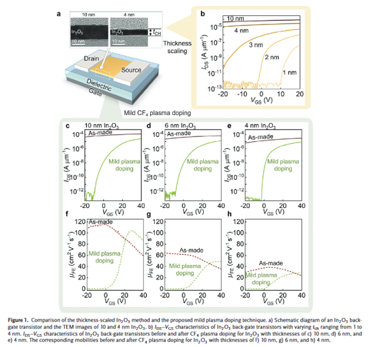
Technology Overview
CF₄ plasma is applied remotely at low power (15 W, 70 °C), causing fluorinated radicals to adsorb onto the In₂O₃ surface, passivating oxygen vacancies and reducing electron density via charge transfer. A subsequent 200 °C anneal forms stable In–F bonds, making the doping permanent. The result: mobility of 104 cm² V⁻¹ s⁻¹ with an Ion/Ioff ratio exceeding 10⁸.
Applications & Benefits
The low thermal budget makes this technique compatible with back-end-of-line (BEOL) processing and monolithic 3D chip integration — areas where silicon's high processing temperatures are prohibitive. The method is demonstrated in functional In₂O₃ depletion-load inverters achieving a voltage gain of 72 V/V, pointing toward practical logic circuits and optoelectronic applications.
Abstract:
Amorphous oxide semiconductors (AOS) are pivotal for next-generation electronics due to their high electron mobility and excellent optical properties. However, In2O3, a key material in this family, encounters significant challenges in balancing high mobility and effective switching as its thickness is scaled down to nanometer dimensions. The high electron density in ultra-thin In2O3 hinders its ability to turn off effectively, leading to a critical trade-off between mobility and the on-current (Ion)/off-current (Ioff) ratio. This study introduces a mild CF4 plasma doping technique that effectively reduces electron density in 10 nm In2O3 at a low processing temperature of 70 °C, achieving a high mobility of 104 cm2 V⁻¹ s⁻¹ and an Ion/Ioff ratio exceeding 10⁸. A subsequent low-temperature post-annealing further improves the critical reliability and stability of CF4-doped In2O3 without raising the thermal budget, making this technique suitable for monolithic three-dimensional (3D) integration. Additionally, its application is demonstrated in In2O3 depletion-load inverters, highlighting its potential for advanced logic circuits and broader electronic and optoelectronic applications.
Breaking the Trade-Off Between Mobility and On–Off Ratio in Oxide Transistors
Author:Chang Yu-Cheng, Wang Sung-Tsun, Lee Yung-Ting, Huang Ching-Shuan, Hsu Chu-Hsiu, Weng Tzu-Ting, Huang Chang-Chang, Chen Chien-Wei, Chou Tsung-Te, Chang Chan-Yuen
Year:2025
Source publication: Advanced Materials, Volume 37, Issue 5, 2413212
Subfield Highest percentage: 99% Mechanical Engineering #3 / 740