Growth of Wafer-Scale Single-Crystal 2D Semiconducting Transition Metal Dichalcogenide Monolayers
In this perspective, we first highlight the growth of single-crystal metal using a single nucleation approach. Then, multi-nucleation growth has been reviewed for growing large domain-size single-crystal 2D TMDs monolayers. Besides, we also outline the re-utilization of the developed metal thin film after detaching successfully grown single-crystal 2D TMD monolayers. In the end, progress and challenges are highlighted.
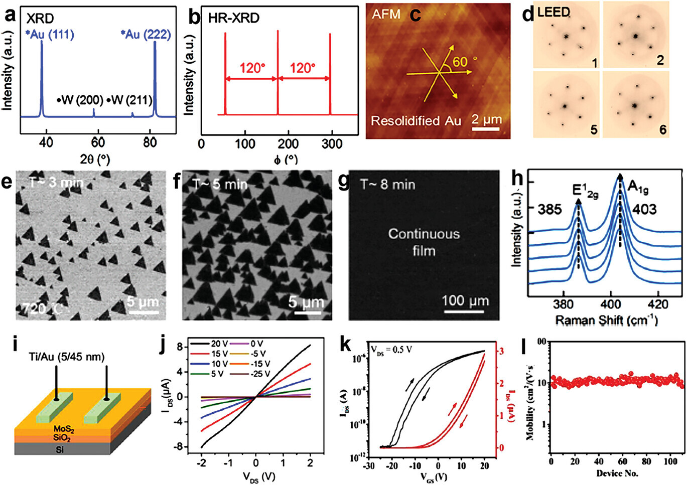
a) XRD pattern of the Au/W foil. b) HR-XRD azimuthal ϕ scans of the off-axis ⟨111⟩ reflection of the Au (111) film. c) AFM image of the re-solidified single-crystal Au (111) substrate. d) LEED pattern of the MoS2 continuous film collected at various positions. e) SEM image of identically oriented small MoS2 domains at the growth time of 3 min. f) SEM image of identically oriented extended MoS2 domains at the growth time of 5 min. g) SEM image of the continuous MoS2 film at the growth time of 8 min. h) Raman spectra of MoS2 film on Au (111)/W film at various positions. i) Schematic of the single-crystal MoS2 FET device. j) IDS-VDS characteristics of the single-crystal MoS2 FET device. k) IDS-VGS curves of the single-crystal MoS2 FET device. l) The distribution of carrier mobilities over 110 FET devices. Reproduced with permission. Copyright 2020 American Chemical Society.
Technology Overview
This paper reviews single and multi-nucleation methods for large-scale 2D TMD preparation. It highlights the challenges of achieving wafer-scale production with single nucleation and emphasizes multi-nucleation as the future, especially with advancements in epitaxial growth on sapphire substrates.
Applications & Benefits
The discussed techniques pave the way for producing high-quality, wafer-scale 2D TMD films. This enables the development of high-performance FET devices with high mobility and ON/OFF ratios, promising commercially viable manufacturing in the near future.
Abstract:
Due to extraordinary electronic and optoelectronic properties, large-scale single-crystal two-dimensional (2D) semiconducting transition metal dichalcogenide (TMD) monolayers have gained significant interest in the development of profit-making cutting-edge nano and atomic-scale devices. To explore the remarkable properties of single-crystal 2D monolayers, many strategies are proposed to achieve ultra-thin functional devices. Despite substantial attempts, the controllable growth of high-quality single-crystal 2D monolayer still needs to be improved. The quality of the 2D monolayer strongly depends on the underlying substrates primarily responsible for the formation of grain boundaries during the growth process. To restrain the grain boundaries, the epitaxial growth process plays a crucial role and becomes ideal if an appropriate single crystal substrate is selected. Therefore, this perspective focuses on the latest advances in the growth of large-scale single-crystal 2D TMD monolayers in the light of enhancing their industrial applicability. In the end, recent progress and challenges of 2D TMD materials for various potential applications are highlighted.
Growth of Wafer-Scale Single-Crystal 2D Semiconducting Transition Metal Dichalcogenide Monolayers
Author:Jitendra Singh, Nadiya Ayu Astarini, Meng-Lin Tsai, Manikandan Venkatesan, Chi-Ching Kuo, Chan-Shan Yang, Hung-Wei Yen
Year:2024
Source publication:Advanced Science, Volume11, Issue11, March 20, 2024
Subfield Highest percentage:99% Biochemistry, Genetics and Molecular Biology (miscellaneous) #1 / 125
https://www.sciencedirect.com/science/article/pii/S0306261924013564